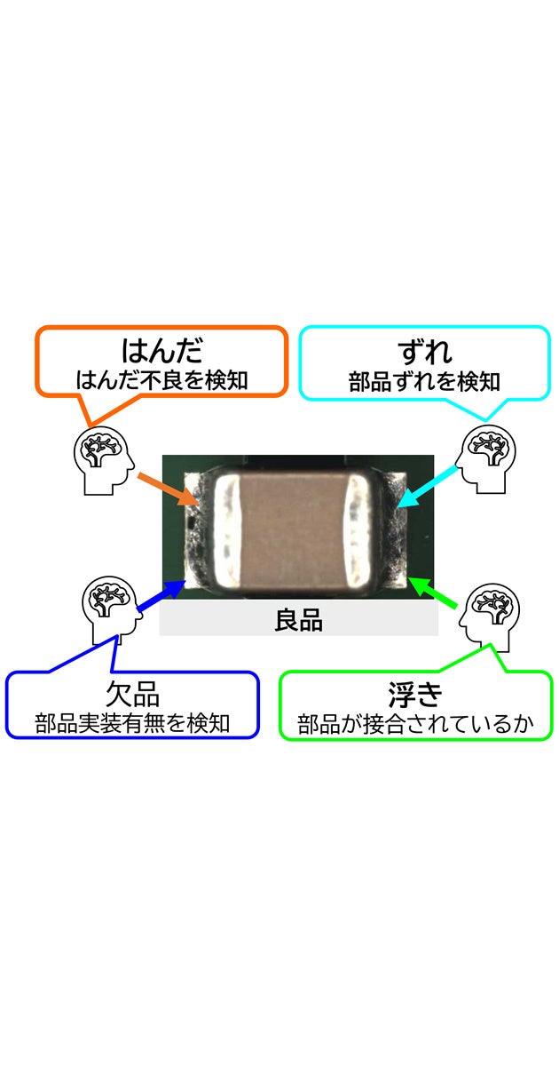
Four Defect Categories Assessed Quickly and Accurately by AI
OKI has developed an AI-based visual inspection technology (hereinafter "this technology") that reduces false detection of solder defects identified during AOI (Automated Optical Inspection) (Note 1) after component mounting on PCBs (printed circuit boards), cutting post-AOI visual inspection time by approximately 80%. Deployment will begin on July 1, 2026, on production lines serving customers of the "Marugoto EMS" service. By training the AI exclusively on good product data (Note 2) and combining proprietary algorithms, this technology shortens visual inspection time while improving inspection accuracy, thereby enhancing customer service quality.
In recent years, driven by the rapid advancement and proliferation of AI, semiconductors mounted on PCBs have become increasingly larger, finer, and multi-layered. In AI servers in particular, numerous large components and ultra-fine pitch components with terminal spacing of just a few microns are mounted, making solder defect detection significantly more challenging.
The newly developed technology integrates OKI's manufacturing expertise for large, high-density PCBs into the AOI system's inspection algorithms, implementing a dedicated AI model for mounted boards. It uses AI to inspect four key defect categories—"solder wetting" (Note 3), "misalignment," "missing components," and "lifting"—enabling fast and highly accurate judgment. Additionally, the system includes a proprietary program that recognizes component-specific characteristics, treating variations such as manufacturing or lot numbers and minor printing smudges—factors that do not affect functionality—as acceptable good products. Furthermore, by adopting a "good product-only learning" approach, which trains the AI using only a small volume of good product data, OKI has optimized the AI technology for high-mix, low-volume production involving tens of thousands of component types and thousands of equipment variants.
Since 2025, OKI has offered the "Marugoto EMS" service, which supports companies in adopting a "manufacturing-without-ownership" business model and improving operational metrics. The introduction of this new technology will contribute to shorter production cycles and higher inspection accuracy in Marugoto EMS customer production. Going forward, OKI will expand the application of this technology to other inspection processes and continue developing new AI-powered systems, broadening AI implementation across diverse manufacturing environments to further enhance production efficiency and quality.
Glossary
Note 1: AOI (Automated Optical Inspection)
Short for Automated Optical Inspection. A machine vision-based recognition technology used to improve upon or supplement manual optical inspection.
Note 2: Good Product-Only Learning
An AI training method that uses only data from good products. Defect detection is performed based on the degree to which inspected items deviate from the learned good product data.
Note 3: Solder Wetting
Refers to the condition where solder properly spreads across the terminal or PCB electrode surface, forming a reliable electrical and mechanical bond.
OKI Electric Industry Co., Ltd. is commonly referred to as OKI.
Company and product names mentioned in this release are generally trademarks or registered trademarks of their respective companies.
Media Inquiries
Public Relations & Promotion Department
Inquiry Form
Customer Inquiries
Industrial Sales Headquarters, EMS Sales Department
Inquiry Form
FACT BOX
- Source: PR TIMES
- Category: 技術開発
- Organizations: OKI