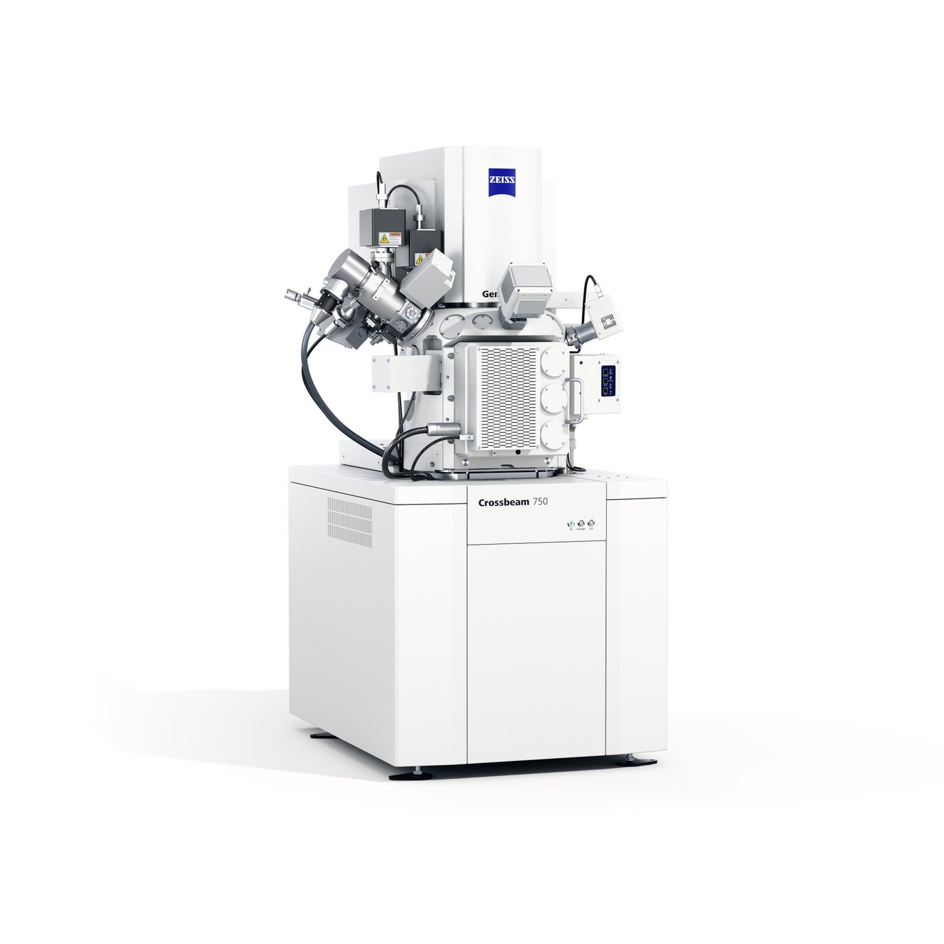
ZEISS Announces New FIB-SEM "Crossbeam 750" Achieving Highly Efficient TEM Lamella Preparation with Live SEM Imaging and High-Resolution Observation with Gemini 4 Electron Optics
ZEISS has announced the new FIB-SEM "Crossbeam 750," which enables highly efficient TEM lamella preparation through advanced live SEM imaging and high-resolution observation using the new Gemini 4 electron optics, significantly improving workflows in various research and inspection fields.
📋 Article Processing Timeline
- 📰 Published: April 2, 2026 at 20:40
- 🤖 AI Analyzed: June 2, 2026 at 12:59 (1456h 19m after Published)
Carl Zeiss Co., Ltd. (Kojimachi, Chiyoda-ku, Tokyo; President and CEO: Vincent Mathieu) globally announced the ZEISS Crossbeam 750, a new focused ion beam scanning electron microscope (FIB-SEM) optimized for high-precision sample preparation, on March 31st, and is now commencing full-scale promotion in Japan.
The new Crossbeam 750 features advanced live SEM imaging capabilities and the newly developed "Gemini 4" electron optics. This allows for extremely clear real-time observation without interrupting FIB (focused ion beam) processing. This dramatically increases the success rate of TEM (transmission electron microscope) lamella preparation for advanced semiconductor device analysis and brings significant efficiency improvements to workflows from R&D to inspection across all fields, from materials science to life sciences.
ZEISS Crossbeam 750 Highlights
◆ Highly efficient TEM lamella preparation through advanced live SEM imaging, enabling clear real-time SEM image observation without interrupting FIB processing.
◆ Significantly improved resolution and S/N ratio at low accelerating voltages with the new ZEISS Gemini 4 electron optics.
◆ Reliable and reproducible workflows achieved by precise and predictable endpoint control, ensuring the preservation of critical structures.
*Watch the video below:
https://zeiss.widencollective.com/assets/share/asset/dvnelneb9g
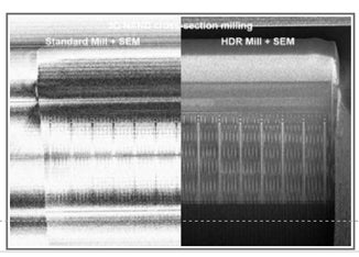
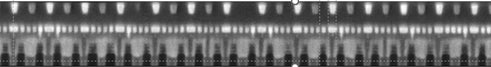
Next-Generation FIB-SEM Born from the Philosophy of "Never Stopping FIB Processing"
"The new ZEISS Crossbeam 750 was designed based on the fundamental principle that customers should not have to interrupt FIB processing to check the processing location within their sample," says Thomas Rogers, Senior Director of Global Market Strategy and Head of the Electronics Business Unit. "The new High Dynamic Range (HDR) Mill+SEM function maintains clear, high-resolution SEM images under all FIB conditions, from high FIB current for fast FIB processing to precise polishing at 0.5kV. Combining this real-time clarity with the Gemini 4 electron optics allows customers to fine-tune the process during processing, enabling the creation of highly uniform TEM lamellae even for first-time samples. This reduces rework and improves yield."
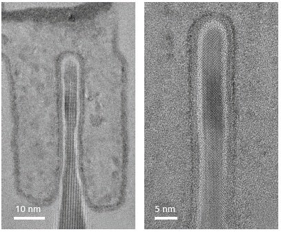
The updated Gemini 4 electron optics enables real-time endpoint setting without background noise and sub-nanometer precision processing control, achieving TEM lamella preparation and accurate 3D analysis. It is an ideal platform for advanced semiconductor analysis, such as analyzing logic and memory devices at cutting-edge nodes, nanofabrication, and 3D volume imaging.
Wide field-of-view observation with reduced image distortion contributes to faster 3D volume imaging acquisition and improved data reliability, supporting the acceleration of scientific discovery.
Reaching the Endpoint on the First Try by "FIB Processing While Observing"
As semiconductor device structures become finer and more complex, high-precision real-time control during FIB processing is essential for analyzing FinFETs, Gate-All-Around (GAA), Complementary FETs (CFETs), and new 2D materials. The ZEISS Crossbeam 750 meets these needs by enabling clear, high-resolution SEM image observation during processing, even under conditions such as low accelerating voltage and tilted samples.
By observing in real-time during the FIB processing, thinning and polishing steps can be optimized on the spot, making it possible to reach nanometer-scale endpoints on the first attempt. This allows for the efficient and predictable production of consistent and excellent TEM lamellae for logic and memory devices at cutting-edge nodes, shortening the lead time to TEM analysis.
Excellent Imaging in Materials Science to Life Sciences Drives Scientific Discovery
The unparalleled capabilities of the ZEISS Crossbeam 750, including consistent TEM lamella preparation, atom probe tomography (APT) sample preparation, nanofabrication (including electron beam lithography), and accurate 3D volume imaging, play a central role in diverse workflows across R&D and inspection departments in all fields. A wide field of view without image distortion and stable low-accelerating voltage observation performance improve the S/N ratio and reduce data acquisition time. Furthermore, standardized unattended operation with high throughput and high-precision positioning capabilities supports advanced workflows.
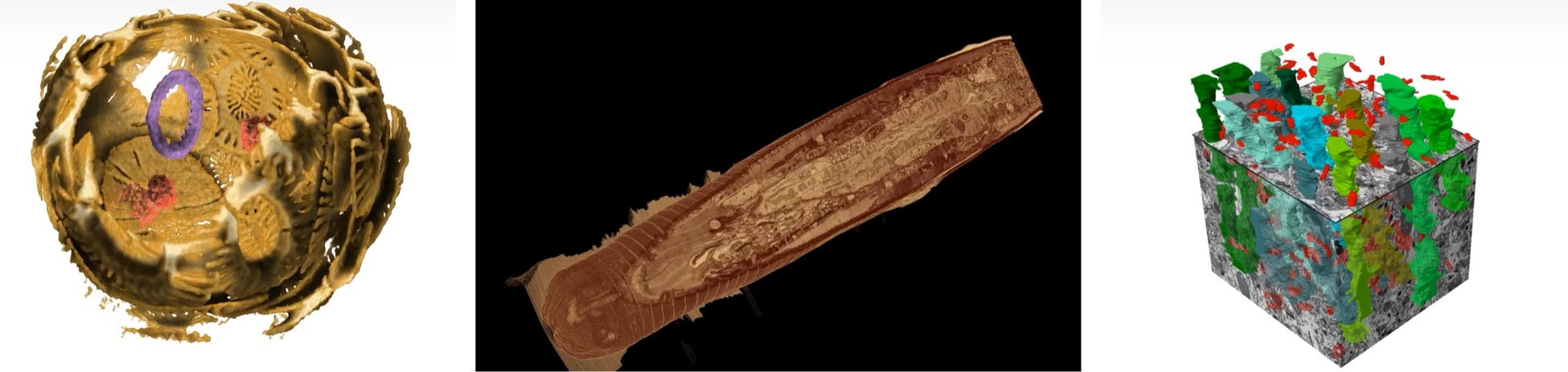
*Watch the videos below:
Left: FIB-SEM Tomography in Life Sciences: Watch the cell biology of algae
Middle: nanotomography_C-elegans_Crossbeam-AURIGA
Right: Ultrastructural investigation of mouse brain utilizing ZEISS
The ZEISS Crossbeam 750, which dramatically improves the TEM lamella preparation workflow, contributes to the advancement of R&D and inspection departments in all fields.
New ZEISS Crossbeam 750
Product page here ↓
https://www.zeiss.com/microscopy/ja/products/sem-fib-sem/fib-sem/crossbeam-750.html
Product video here ↓
https://zeiss.widen.net/s/vghvxjxq9z/crossbeam-750_product-video_v004_final
About ZEISS
ZEISS is an internationally leading technology enterprise operating in the fields of optics and optoelectronics, founded in Germany in 1846. In Japan, there are three legal entities established in 1911: Carl Zeiss Co., Ltd., Carl Zeiss Meditec Co., Ltd., and Carl Zeiss Vision Japan Co., Ltd. The company operates in four segments (Semiconductor Manufacturing Technology, Industrial Quality & Research, Medical Technology, and Consumer Markets) and is a global enterprise with sales of approximately 12 billion euros (as of September 2025). It provides innovative solutions in various fields such as industrial metrology, quality assurance, life sciences, materials research, ophthalmology, and microsurgery, earning high recognition worldwide.
ZEISS positions innovation as its growth driver, investing approximately 15% of its revenue in research and development annually. With approximately 46,600 employees, 40 R&D facilities, around 30 production sites, and about 60 sales and service companies, it operates in approximately 50 countries (as of September 2025). Furthermore, its owner, the Carl Zeiss Foundation, is one of Germany's largest foundations dedicated to advancing science.
About Carl Zeiss Co., Ltd. Research Microscopy Solutions (Microscopy Division)
Research Microscopy Solutions (RMS) is a business unit that develops, manufactures, and sells microscopes primarily for research. It offers a wide range of solutions, including optical, electron, and X-ray microscopy systems, correlative microscopy, and AI-powered software, for life sciences, materials, industrial research, and education.
FAQ
What are the main features of the ZEISS Crossbeam 750?
Key features include real-time observation during FIB processing via live SEM imaging, high-resolution imaging with the new Gemini 4 electron optics, and precise endpoint control.
What application areas are expected for this product?
It is expected to be used in advanced semiconductor device analysis, materials science, and life sciences for TEM lamella preparation, atom probe tomography, and 3D volume imaging.
How has it evolved compared to conventional FIB-SEM?
A significant advancement is the ability to observe clear SEM images in real-time during FIB processing without interruption. This dramatically improves the success rate and efficiency of TEM lamella preparation.