March 31, 2026 Patentix Inc. (hereinafter referred to as "the Company") has successfully fabricated a depletion-type MOSFET using rutile-type germanium dioxide (r-GeO₂), a material attracting attention as a next-generation power semiconductor, and has demonstrated its transistor operation. MOSFETs are fundamental power devices, and this achievement is a crucial step towards the realization of future enhancement-type MOSFETs.
【Background】 Rutile-type germanium dioxide (r-GeO₂) possesses a larger bandgap (4.68 eV) than silicon carbide (SiC) or gallium nitride (GaN). Theoretical predictions suggest it can exhibit both p-type and n-type conductivity, making it a promising next-generation semiconductor material for realizing high-voltage, high-power, and high-efficiency power semiconductor devices.
The Company has previously established technologies for depositing n-type r-GeO₂ with antimony (Sb) as a dopant and controlling its conductivity. This has led to the realization of ohmic contacts through n+ layer deposition [1] and the successful demonstration of Schottky barrier diode (SBD) operation through n-layer deposition [2]. Meanwhile, the early realization of MOSFETs, another fundamental power device, has been highly anticipated.
【Previous Research】 Previous research on r-GeO₂ MOSFETs includes a report on FET operation by forming a GeO₂ film on a SiO₂/p+ Si substrate using sputtering deposition [3]. Furthermore, in November 2025, MOSFET operation was confirmed in r-GeO₂ single crystals grown by the TSSG method with phosphorus ion implantation. However, the demonstration of MOSFET operation using heteroepitaxial films, which are expected to offer advantages in terms of large substrate areas and cost competitiveness, had not been reported until now.
【Results】 Leveraging the deposition technologies established by the Company, we have now successfully demonstrated the transistor operation of a depletion-type MOSFET that can be fabricated solely with n-type r-GeO₂.
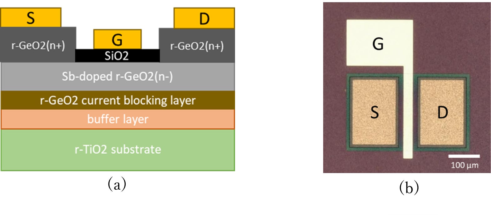
Figures 1(a) and 1(b) show a schematic cross-section and an optical micrograph of the fabricated r-GeO₂ MOSFET. A current blocking layer was formed using a doped r-GeO₂ film on an r-TiO₂ substrate. Subsequently, an Sb-doped n-channel layer (thickness 160 nm) and source/drain n+ layers were deposited via selective growth, resulting in a MOSFET with a device isolation structure and reduced ohmic contact resistance. The gate insulating film used was SiO₂ (thickness 75 nm), and Pt/Ti was used for the electrodes. In this device structure, applying a negative gate voltage extends the depletion layer directly beneath the gate insulating film, thereby blocking the current path between the drain and source and turning the current off.
Figure 1: (a) Schematic cross-section and (b) optical micrograph of the r-GeO₂ MOSFET
Figure 2(a) shows the ID-VG characteristics of the fabricated r-GeO₂ MOSFET. The drain current (ID) varied over five orders of magnitude with the gate voltage (VG), confirming depletion-type transistor operation where the drain current turns off with a negative gate voltage. The hysteresis measurement shown in the same figure indicates minimal characteristic variation with gate voltage application, suggesting the formation of a gate insulating film interface with few defects, even without process condition optimization.
Furthermore, the ID-VD characteristics shown in Figure 2(b) confirm typical behavior transitioning from linear to saturation characteristics as the drain voltage (VD) increases.
Figure 2: (a) ID-VG characteristics and (b) ID-VD characteristics of the r-GeO₂ MOSFET
【Future Prospects】 To demonstrate the utility of r-GeO₂ as a power semiconductor material, we will focus on establishing fabrication technology for p-type r-GeO₂ and proceed with studies towards demonstrating the operation of enhancement-type MOSFETs utilizing this technology.
[1] Y. Shimizu, et al., N-type conductivity in single-phase r-GeO₂ thin films., 2024 MRS Fall Meeting & Exhibit, SF04.15.08 (2024).
[2] Y. Shimizu, et al., "Schottky Barrier Diode Characteristics of Rutile Structure Germanium Dioxide (r-GeO₂)", The 72nd Annual Meeting of the Japan Society of Applied Physics, 15a-K403-11 (2025).
[3] D. Dai, et al. "Demonstration of enhancement-mode high-k gated field-effect transistors with a novel ultrawide bandgap semiconductor: Germanium oxide." APL Materials 13.7 (2025).
[4] K. Tetzner, et al. "Lateral rutile GeO₂ MOSFET devices on single-crystal r-GeO₂ substrates." IEEE Electron Device Letters (2025).
FACT BOX
- Source: PR TIMES
- Category: New Product
- Products / services: r-GeO₂ MOSFET