[Osaka Institute of Technology] Challenging Next-Generation Semiconductor Devices with Two-Dimensional Materials
Osaka Institute of Technology has released the 18th installment of its "Research Power" web series, featuring Professor Akira Fujimoto's research on developing next-generation semiconductor devices using ultra-thin two-dimensional materials. This work aims to overcome the miniaturization limits of silicon and create more power-efficient electronic components. The series makes cutting-edge research accessible through an easy-to-understand conversational format.
📋 Article Processing Timeline
- 📰 Published: April 2, 2026 at 23:00
- 🔍 Collected: April 2, 2026 at 19:37
- 🤖 AI Analyzed: April 17, 2026 at 08:13 (348h 35m after Collected)
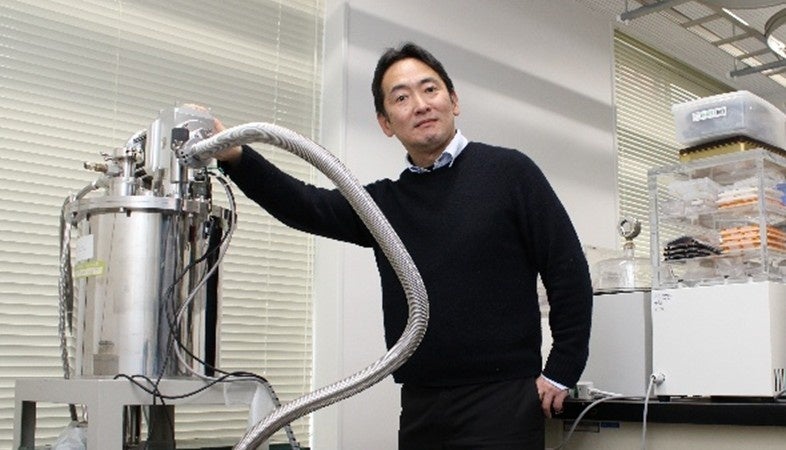
Osaka Institute of Technology (President: Susumu Inoue) released the 18th installment of its web series "Research Power," which introduces cutting-edge research from the university on its homepage under "Lab VOICE," today. This installment introduces the development of next-generation semiconductor devices using "two-dimensional materials," an ultra-thin substance, led by Professor Akira Fujimoto of the General Education Department.
1. Faculty Member: Professor Akira Fujimoto
2. Affiliation: General Education Department
3. Theme: Challenging Next-Generation Semiconductor Devices with Two-Dimensional Materials
4. URL: https://www.oit.ac.jp/lab_voice/18_T-hujimoto.html
【Research Overview】
With the increasing number of electronic devices such as smartphones and personal computers, the amount of electricity used is growing. Therefore, there is a demand for machines and components that operate with as little power as possible. While devices are continuously being miniaturized to improve performance, it is becoming difficult to further miniaturize conventional silicon materials. As an alternative material, two-dimensional materials are gathering much attention.
Professor Fujimoto is working on applying two-dimensional materials, such as graphene, to semiconductor devices (elements using semiconductor materials) and gas sensors. In transistors fabricated by combining graphene and molybdenum disulfide, it was confirmed that the properties can be significantly altered by the material combination, providing crucial insights that could lead to the development of high-performance semiconductor devices.
【Web Series "Research Power"】
● Explains cutting-edge research in an easy-to-understand manner using a conversational style with frequent use of figures and videos.
● Introduces one faculty member per month from the university's 200 laboratories.
※ The titles and URLs of the 5 most recent installments from the past "Research Power" series are introduced below.
【 "Research Power" Back Numbers 】
Deciphering the Moon and Stars Depicted in Ancient Art from an Astronomical Perspective
Professor Kiyoshi Matsuura, Faculty of Engineering, Department of General Human Sciences
https://www.oit.ac.jp/lab_voice/20250730.html
Correcting the Serving Motion of Tennis Beginners with Generative AI
Associate Professor Masataka Seo, Faculty of Robotics and Design Engineering, Department of Systems Design Engineering
https://www.oit.ac.jp/lab_voice/13_S-seo.html
Considering Power Supply Systems Where Renewable Energy Thrives
Lecturer Hidenori Matayoshi, Faculty of Engineering, Department of Electrical and Electronic Systems Engineering
https://www.oit.ac.jp/lab_voice/15_E-matayoshi.html
Aiming for Lunar Exploration with Hopping Robots
Professor Kosei Taniguchi, Faculty of Robotics and Design Engineering, Department of Robotics Engineering
https://www.oit.ac.jp/lab_voice/16_R-taniguchi.html
Developing "Edge AI" that Runs Swiftly and Intelligently on Devices
Professor Chikako Nakanishi, Faculty of Information Science, Department of Intelligent Information Engineering