AMD: 'Venice' EPYC Processor in Mass Production with TSMC's 2nm Process, to Expand to US Fab in Future
U.S. chip giant AMD announced on May 21st that its EPYC processor, codenamed 'Venice,' has entered mass production in Taiwan using TSMC's 2nm process technology. There are also plans to mass-produce it at TSMC's Arizona fab in the future. This move aims to accelerate the development of next-generation AI infrastructure and strengthens AMD's geographically diverse advanced manufacturing layout. The company also plans to extend the 2nm technology to its 6th generation EPYC processor, 'Verano'.
📋 Article Processing Timeline
- 📰 Published: May 21, 2026 at 16:56
- 🔍 Collected: May 21, 2026 at 17:01 (5 min after Published)
- 🤖 AI Analyzed: May 21, 2026 at 17:23 (21 min after Collected)
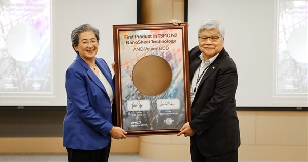
(CNA, Hsinchu, May 21, by reporter Chang Chien-chung) U.S. chip maker Advanced Micro Devices (AMD) announced today that its EPYC processor, codenamed 'Venice,' has entered mass production in Taiwan using TSMC's 2-nanometer process technology, with plans to expand mass production to TSMC's fab in Arizona, USA, in the future.
In a press release today, AMD Chair and CEO Lisa Su stated that advancing the mass production of Venice on TSMC's 2nm process technology is a significant step in accelerating the development of next-generation AI infrastructure. As AI and agent-based workloads expand rapidly, customers need platforms that can move from innovation to mass production more quickly. The deep collaboration with TSMC helps AMD bring leading computing technology to market at the speed and scale that current demand requires.
AMD pointed out that the mass production of Venice in Taiwan, along with future capacity expansion plans at TSMC's Arizona fab, reflects AMD's continuous strengthening of its geographically diverse advanced manufacturing layout. By combining the technological innovations of the next-generation EPYC processor with global advanced capacity, AMD continues to expand its solid foundation to help customers deploy and scale their AI infrastructure.
TSMC Chairman and President C.C. Wei said that the close collaboration with AMD reflects the importance of combining leading process technology with advanced design innovation in driving the development of next-generation high-performance and AI computing.
AMD stated it plans to extend TSMC's 2nm process technology to 'Verano' in its data center central processing unit (CPU) roadmap, which is the 6th generation EPYC processor, to create industry-leading performance-per-dollar-per-watt.
AMD noted that Verano is designed to support cloud and AI computing workloads and is expected to introduce advanced memory innovations, including LPDDR, on top of the EPYC platform. This will provide the necessary CPU performance, bandwidth, and power efficiency for increasingly power-constrained workloads and applications.
AMD said its collaboration with TSMC covers key technologies required to expand modern data center computing, from TSMC's 2nm process technology for next-gen CPUs to advanced packaging technologies, including TSMC's SoIC-X and CoWoS-L.
FAQ
AMD最新宣布量產的處理器是什麼?採用了什麼技術?
AMD宣布代號為「Venice」的EPYC處理器已採用台積電的2奈米製程技術在台灣量產。
「Venice」處理器除了在台灣生產,還有其他生產計畫嗎?
是的,AMD計劃未來將「Venice」處理器的生產擴展到台積電位於美國亞利桑那州的晶圓廠。
這次合作對AMD的戰略佈局有何意義?
此舉反映了AMD持續強化其地理多元的先進製造佈局,並透過結合技術創新與全球產能,協助客戶部署和規模化AI基礎設施。
AMD未來的產品藍圖中還有什麼規劃?
AMD計劃將台積電的2奈米製程技術延伸至其第6代EPYC處理器,代號為「Verano」,專為支援雲端與AI運算工作負載而設計。
台積電對這次與AMD的合作有何看法?
台積電董事長暨總裁魏哲家表示,這次緊密合作反映了在推動下一代高效能與AI運算發展中,結合領先製程技術與先進設計創新的重要性。