CNA reporter Chao Min-Ya Taipei, 16th) A new semiconductor inspection technology developed by a Taiwanese team has overcome the limitations of relying solely on theoretical simulations, providing crucial experimental evidence for the miniaturization of next-generation semiconductor components. The team stated that this technology offers a more accurate method for assessing the quality of component contacts, and they are currently in discussions with industry players to shorten the verification cycle from research and development to process integration.
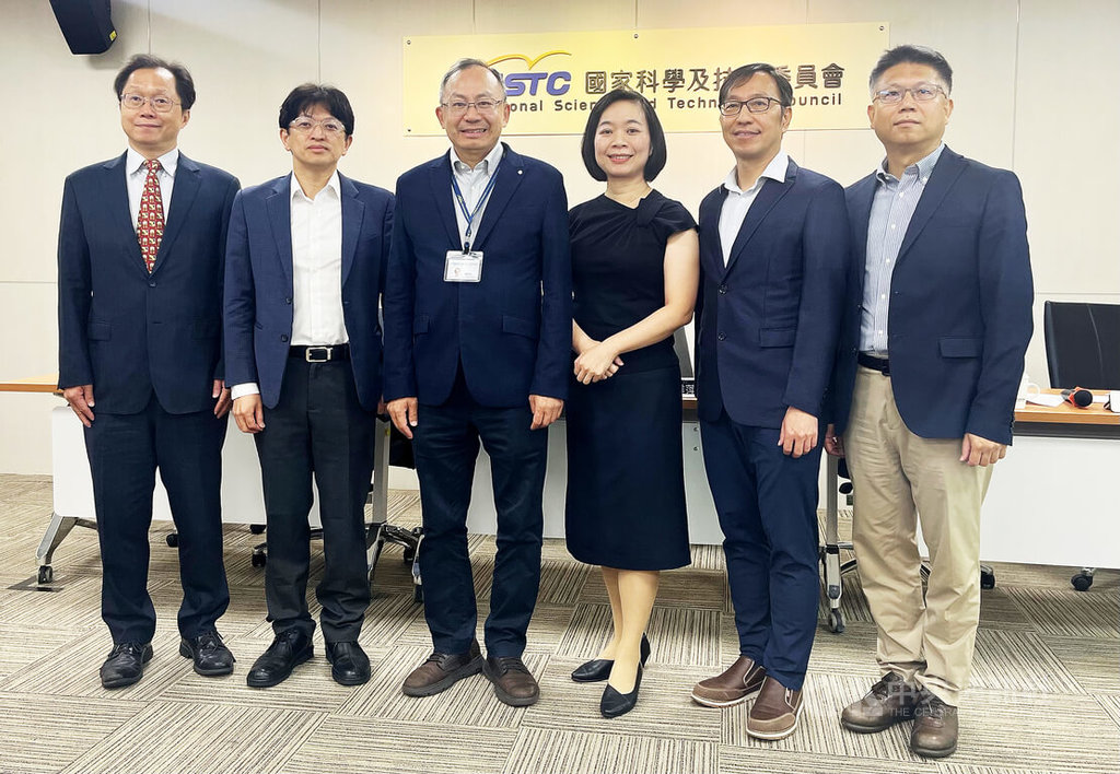
The National Science and Technology Council (NSTC) held a press conference today to announce the research results. With the support of the NSTC, Professor Chiu Ya-Ping from the Department of Physics at National Taiwan University led the development of this new semiconductor inspection technology in collaboration with Professor Lan Yen-Wen from the Department of Physics at National Taiwan Normal University and Professor Lee Lien-Chung from the National University of Singapore. This technology enables direct measurement of the electron transfer length at the metal/semiconductor contact edge with atomic-level spatial resolution in the actual operating state of advanced two-dimensional semiconductor transistor components, providing an important detection breakthrough for evaluating the potential of transistor miniaturization.
The NSTC pointed out that with the increasing demand for high-performance, low-power chips, the continuous miniaturization of semiconductor components has become a core issue in global technological development. Two-dimensional semiconductors, with their atomic-level thickness and superior gate control capabilities, are considered important candidate materials for continuing the miniaturization of advanced logic components in the post-Moore era. However, whether transistors can continue to be miniaturized and applied to future chip technology depends not only on the channel length but also on the quality of the metal contact area.
Professor Chiu explained that the contact edge is a critical region where electrons are injected from the metal electrode into the semiconductor channel. The electron transfer length is the effective length required for electrons to complete injection at the contact edge, directly determining the size of the contact resistance and the efficiency of electron injection. It is also an important indicator of whether the component can maintain normal operation under extreme miniaturization conditions, thereby affecting the component's current output and power consumption performance.
She stated that the assumptions relied upon by traditional theoretical models are often not applicable in advanced two-dimensional semiconductor transistor systems and cannot directly present the true spatial electron transmission behavior at the contact interface. This breakthrough is based on Taiwan's accumulated technology in the field of cross-sectional scanning microscopy. The team further integrated the in-situ operation bias function into the measurement system, enabling direct detection of electron transmission behavior at the contact edge between metal and semiconductor with atomic-level spatial resolution under the actual operating state of the component.
Professor Chiu said that this technology is like setting up a high-resolution camera at the atomic scale on the metal and semiconductor contact edge, allowing researchers to directly observe how electrons cross the contact edge during the component's operation and precisely measure the effective electron transfer length. From the past where only theoretical estimates of length were possible, it is now possible to verify through experiments, providing direct data for the miniaturization research of next-generation semiconductor components.
She pointed out that the team has also extended this measurement method to silicon-on-insulator (SOI) components, proving that this technology is not only applicable to two-dimensional semiconductors but also has the potential to serve as a universal analysis platform for studying the contact characteristics of various advanced semiconductor components.
Professor Chiu stated that the research results have been published in the top international academic journal 'Nature', and the team is in discussions with industry players, accepting samples from companies for testing and continuously improving the technology, with the goal of helping the industry accelerate the verification cycle.
The NSTC pointed out that this research, from the development of detection technology, method establishment to the verification of advanced components, was entirely led and completed by the Taiwanese research team, demonstrating Taiwan's self-developed capabilities and international leading strength in the field of key measurement technologies for forward-looking semiconductors. (Editor: Lin Shu-Yuan) 1150716
Stand with facts, your every sponsorship is the power to safeguard press freedom
Download the CNA 'First-Hand News' app to stay updated with the latest news
The text, images, and videos on this website may not be reproduced, publicly broadcast, or publicly transmitted and utilized without authorization.
FACT BOX
- Source: CNA (Central News Agency)
- Category: 研究