Industry-Academia Collaboration Project Utilizing NDA-Free PDK for Actual Chip Manufacturing Kicks Off
Tokai Rika Co., Ltd., Kyushu University, AIST Solutions Co., Ltd., and OpenSUSI, a general incorporated association, have launched a 5-year joint project for semiconductor human resource development and implementation verification, utilizing NDA-free PDK for actual chip manufacturing. The project's key feature is providing hands-on experience from design to chip manufacturing in an open design environment. In 2025, a hands-on seminar was held at Kyushu University, and actual chip manufacturing was conducted with technical cooperation from Tokai Rika. The project is now recruiting participants to strengthen the human resource base for the future semiconductor industry.
📋 Article Processing Timeline
- 📰 Published: April 10, 2026 at 18:00
- 🔍 Collected: April 10, 2026 at 09:01
- 🤖 AI Analyzed: April 16, 2026 at 01:32 (136h 30m after Collected)
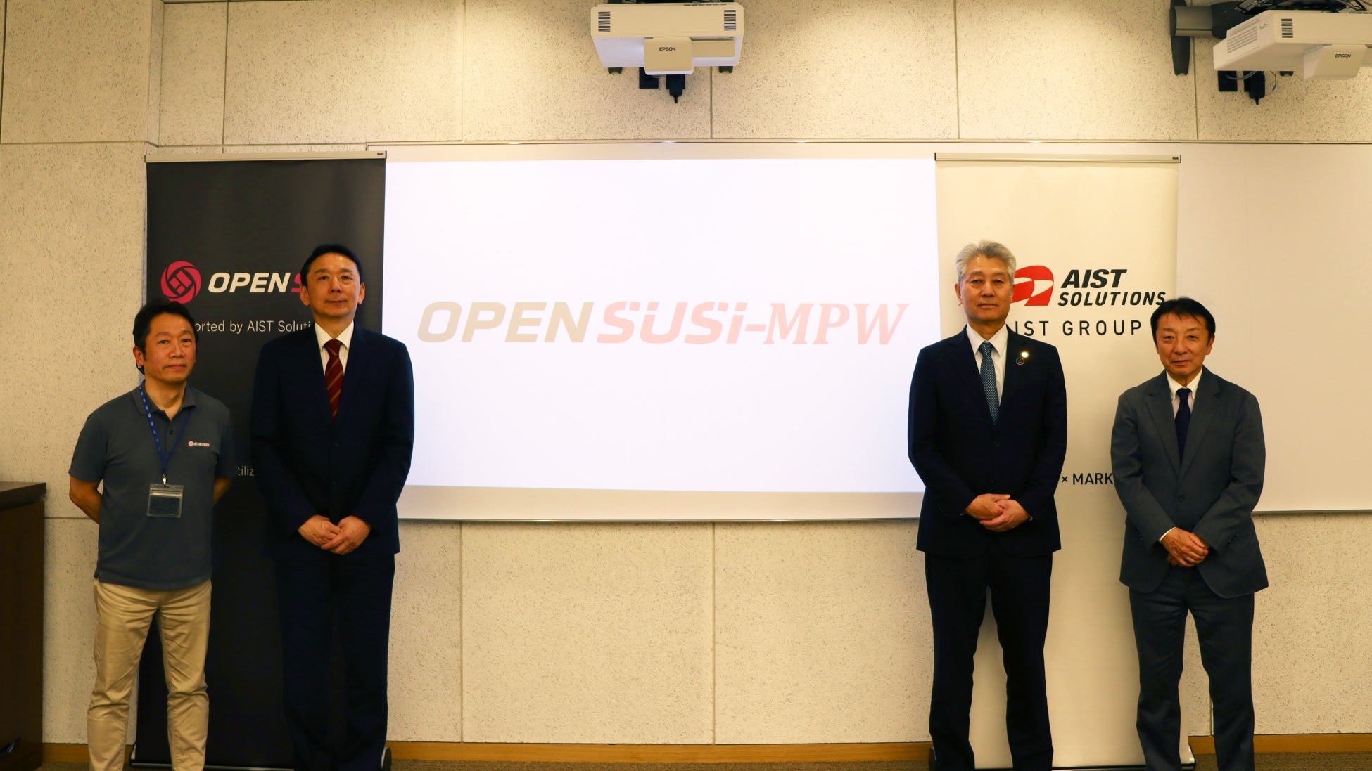
Tokai Rika Co., Ltd., National University Corporation Kyushu University, AIST Solutions Co., Ltd., and OpenSUSI, a general incorporated association, held a kick-off ceremony for a 5-year joint project in 2026. This industry-academia collaboration project aims to develop semiconductor human resources and verify implementation through actual chip manufacturing, utilizing PDK (Process Design Kit) that does not rely on NDA (Non-Disclosure Agreements).
The biggest feature of this project is that it allows participants to experience the entire process from design to chip manufacturing in an open design environment using NDA-free PDK.
▪️Project Overview
This project is promoted by the four parties in collaboration, with the aim of both fostering immediately effective human resources in the semiconductor field and verifying implementation tailored to industrial needs. The biggest feature is the adoption of NDA-free PDK. This makes it possible to engage in practical chip manufacturing processes without excessive restrictions, even in university education and industry-academia collaboration settings.
2025 Achievements:
Hands-on seminars were conducted at Kyushu University. Students and young engineers experienced semiconductor design to complete chip manufacturing using NDA-free PDK.
Actual chip manufacturing was carried out with technical cooperation from Tokai Rika. The process from design input to manufacturing completion was demonstrated.
AIST Solutions / OpenSUSI prepared and provided an environment where design can be done using NDA-free PDK.
■ 2026 Positioning and Future Developments
2026 is positioned as the first year of full-scale deployment for this 5-year project. Based on an open design and manufacturing environment utilizing NDA-free PDK, the following initiatives will be continued and developed:
Continuation and advancement of hands-on semiconductor human resource development
Provision of opportunities for actual chip manufacturing and verification using NDA-free PDK
Establishment of a practical and highly reproducible education and implementation model through industry-academia collaboration
As compensation for financial support for this program, corporate logos will be embedded in prototype chips to raise awareness of semiconductor design human resource development as a social contribution activity.
By establishing an environment where education and implementation are not separated, and participants can experience the entire process from design to chip completion, we aim to strengthen the human resource base that will support the future semiconductor industry.
■ Recruitment of Participants
This project is currently recruiting participants who are engaged in semiconductor design at universities or technical colleges and aim to play an active role in the semiconductor field in the future. We also welcome individuals belonging to companies who agree with this initiative and wish to work together on semiconductor design to actual chip manufacturing as a new business in the future.
If you are interested in this matter, please contact us at:
▶︎ Contact: OpenSUSI Secretariat secretary@opensusi.org
FAQ
What is the main purpose of this industry-academia collaboration project?
The main purpose is to achieve both the development of immediately effective human resources in the semiconductor field and the verification of implementation tailored to industrial needs.
What is NDA-free PDK?
NDA-free PDK (Process Design Kit) does not rely on Non-Disclosure Agreements, enabling hands-on experience from semiconductor design to chip manufacturing in an open environment.